Jeong Ho Lyu's Email & Phone Number
Chief Architect/Camera Lead at Baidu USA
Jeong Ho Lyu Email Addresses
Jeong Ho Lyu's Work Experience


Maru LSI
Principal Engineer
September 2005 to May 2008


Show more
Show less
Jeong Ho Lyu's Education
Seoul National University
Ph. D, Electronics Engineering
April 1993 to April 1997
Show more
Show less
Frequently Asked Questions about Jeong Ho Lyu
What company does Jeong Ho Lyu work for?
Jeong Ho Lyu works for Baidu USA
What is Jeong Ho Lyu's role at Baidu USA?
Jeong Ho Lyu is Chief Architect/Camera Lead
What is Jeong Ho Lyu's personal email address?
Jeong Ho Lyu's personal email address is j****[email protected]
What is Jeong Ho Lyu's business email address?
Jeong Ho Lyu's business email address is jeongho.lyu@***.***
What is Jeong Ho Lyu's Phone Number?
Jeong Ho Lyu's phone (213) ***-*351
What industry does Jeong Ho Lyu work in?
Jeong Ho Lyu works in the Internet industry.
Jeong Ho Lyu's Professional Skills Radar Chart
Based on our findings, Jeong Ho Lyu is ...
What's on Jeong Ho Lyu's mind?
Based on our findings, Jeong Ho Lyu is ...
Jeong Ho Lyu's Estimated Salary Range
Jeong Ho Lyu Email Addresses
Find emails and phone numbers for 300M professionals.
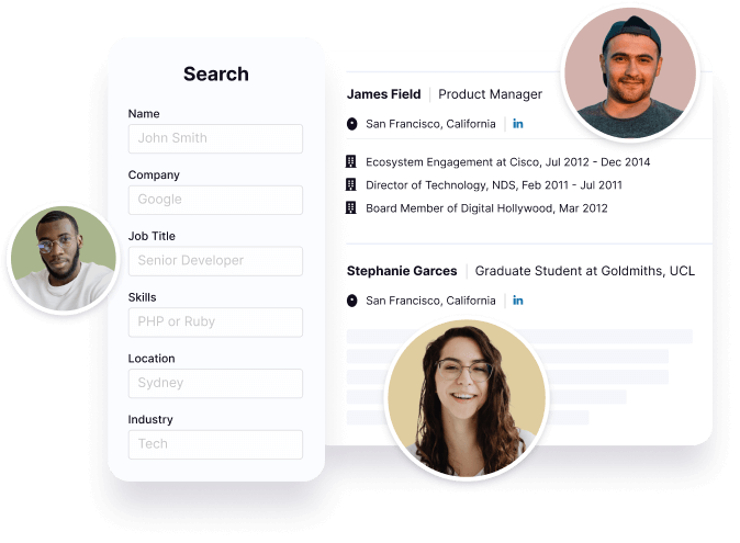
Search by name, job titles, seniority, skills, location, company name, industry, company size, revenue, and other 20+ data points to reach the right people you need. Get triple-verified contact details in one-click.In a nutshell
Jeong Ho Lyu's Ranking
Ranked #833 out of 16,660 for Chief Architect/Camera Lead in California
Jeong Ho Lyu's Personality Type
Introversion (I), Sensing (S), Thinking (T), Perceiving (P)
Average Tenure
2 year(s), 0 month(s)
Jeong Ho Lyu's Willingness to Change Jobs
Unlikely
Likely
Open to opportunity?
There's 91% chance that Jeong Ho Lyu is seeking for new opportunities
People you may be
interested in

Autonomous Vehicle Operations Lead at Baidu USA

Senior staff software engineer/researcher at Baidu USA
Director & Head of Hardware at Baidu USA
Vice President of Client Development at The Trade Desk

Operations General Manager at Planet Fitness

Public Speaker at Anthony Morrison

Co-Founder, CEO at The Meet Group

Founder & CEO at Drone Energy

Team Lead at Infoverity

Founder | Chief Executive Officer at Sootchy Inc

Lead Implementation Analyst at MCG Health

Farmer/Owner at Shirttail Creek Farm


Jeong Ho Lyu's Social Media Links
/in/jeong-ho-lyu-24608011 /company/baidu-usa /school/%ec%84%9c%ec%9a%b8%eb%8c%80%ed%95%99%ea%b5%90-seoul-national-university-/